ADC转换器参考电压模块的版图设计(26000字)
摘 要
版图设计是决定良率高低的一个重要环节,按设计自动化程度来分,可将版图设计方法分成手工设计和自动设计两大类。按照对布局布线位置的限制和布局模块的限制来分, 则可把设计方法分成全定制和半定制两大类。由于制造工艺水平的提高,特征尺寸的减小,各种寄生参数对电路的影响也越来越大,在版图设计中有越来越多的问题要考虑。
本文首先是分析比较了各种高速模数转化器的特点之后采用Cadence公司的Virtuoso定制设计平台,使用全定制的的方法对一个ADC参考电压电路进行版图设计,ADC参考电压电路使用了cmos工艺,量程为0.5V,在版图时调用Cadence公司提供的90nm标准cmos工艺库,用Spectre工具对电路进行了性能分析和仿真,并在Cadence公司提供的工艺文件下完成了版图设计,详细的分析了版图设计的过程,介绍了DRC规则和LVS,然后使用Assura工具进行DRC和LVS验证,进行仿真的验证,证明本论文的版图设计完全符合要求。在最后还对一些DRC和LVS错误进行了分析。
关键词:参考电压电路 版图设计 cmos 工艺 全定制 后仿真
Abstract
Layout design is an important part of the rate decision according to the degree of automation design, and layout design methods can be divided into the design manual and automatic design of two categories. According to the place and route location and layout of the restrictions to limit the sub-module, the design methods can be divided into full-custom and semi-custom two categories. Since raising the level of manufacturing technology, feature size decreases, the various parameters on the circuit parasitic effects also growing in the territory of the design of a growing number of issues to consider.
This paper is a comparative analysis of the characteristics of digital converter using Cadence Virtuoso company, use the custom design platform for a method of customized reference voltage circuit ADC layout design,. ADC reference voltage circuit to maintain the use of the cmos technology, Range for 0.5 V, called the Cadence companies to provide standard cmos 90 nm process for using the tools Spectre circuit performance analysis and simulation, and Cadence technology companies to provide the documents to complete the layout, a detailed analysis of the layout design process, the DRC rules are introduced and use of Assura Tools DRC and LVS verification,and simulation test to prove that the layout of the paper fully meet the requirements. In the end, some mistakes of LVS DRC and analyzed.
Key Words:reference voltage circuit layout design cmos technology full-custom post layout simulation.
目 录
摘 要 I
Abstract II
1绪论 1
1.1本课题研究的意义 1
2版图设计方案 2
2.1版图设计工具简介 2
3模拟数字转换器(ADC)简介 3
3.1工作原理 3
3.2模数转换器的种类 4
3.2.1全并行结构模数转换器 5
3.2.2两步式模数转换器 6
3.2.3流水线模数转换器 8
3.2.4流水线模数转换器的体系结构 9
4电路分析 11
4.1参考电压电路 11
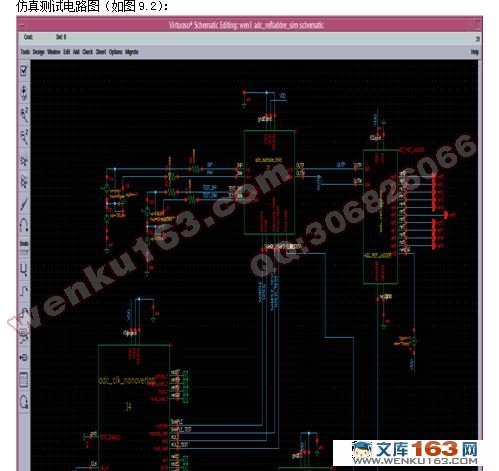
4.2电路模拟仿真结果 11
5版图设计 14
5.1 CMOS工艺概述 14
5.2单元版图设计 15
5.2.1 90nm制造工艺综述 15
5.2.2电容的版图设计 16
5.2.3 MOS管的版图设计 17
5.2.4电阻的版图设计 19
5.3CMOS保护环设计 20
5.4天线效应的分析 21
5.5衬底噪声分析 22
5.6 MOS管的匹配分析 23
5.7版图的总体设计 23
5.7.1估算芯片面积 23
5.7.2电源规划 27
5.7.3 布局 28
5.7.4 布线 29
5.7.5 版图优化 31
5.8版图 35
6物理验证 38
6.1设计规则检查 38
6.1.1 DRC规则介绍 38
6.1.2 DRC操作 41
6.2 电路规程检查 43
6.2.1 LVS介绍 43
6.2.2 LVS操作 44
7版图错误分析 46
7.1DRC错误分析 46
7.1.1 OXIDE.X.1错误 46
7.1.2 METAL1.SP.1.2错误 47
7.1.3 CONT.W.1错误 48
7.2 LVS错误分析 49
8总结及讨论 51
参考文献 52
附 录 53
致 谢 55
|