ZnO:Sb纳米结构的光电性能研究
来源:wenku163.com 资料编号:WK1639383 资料等级:★★★★★ %E8%B5%84%E6%96%99%E7%BC%96%E5%8F%B7%EF%BC%9AWK1639383
资料介绍
ZnO:Sb纳米结构的光电性能研究(含任务书,开题报告,外文翻译,毕业论文8900字,答辩PPT)
摘 要
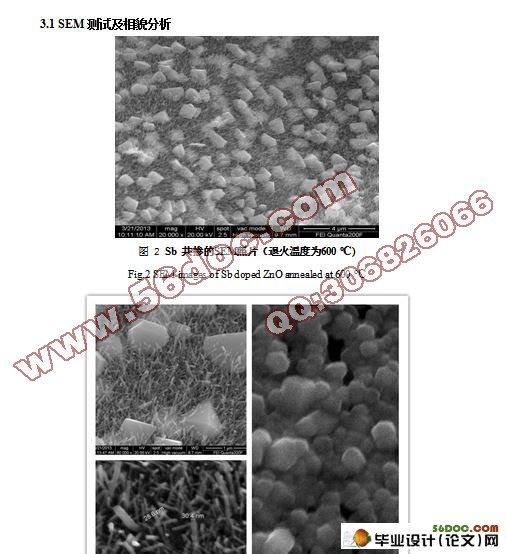
用硝酸锌为主要原料,掺杂锑,探讨了用溶胶自蔓延燃烧法合成纳米级ZnO:Sb光电材料的制备工艺;用扫描电子显微镜(SEM)对产物形貌进行表征,然后对合成产物的光电导性质进行深入的研究。结果表明:退火温度为600 oC左右的条件下,在条带状的结构的ZnO: Sb表面生长出直径约为30 nm的纳米棒,掺杂元素Sb均已进入到ZnO晶格中,形成了六角纤锌矿结构且具有高度的C轴择优取向。光电导测试中,产生最大光电流的峰值波长大约为355 nm,且光强不同响应也不同。发生光电效应时,在入射光频率一定的条件下,饱和光电流与入射光强成正比。 当光照突然中止时,产生的光载流子需要一段时间消失,光载流子消失所需要的时间为弛豫时间。光强增大,相当于光子数量增大,产生的光电子数量跟着增大。
关键词:氧化锌纳米结构;光电导;锑掺杂
Research on Photoelectric Properties of Sb-doped ZnO Nanostrutures
Abstract
Using Zn(NO3)2 as precursor and Sb as dopants, the preparation technology of nanostructure ZnO : Sb photovoltaic materials using Sol-gel Auto-combustion process has been discussed. It was indicated that the striped nanometer ZnO : Sb nanorods can be synthesized when annealed at 600 oC, whose particle diameter is about 30 nm, and peak wavelength generating maximum photocurrent is about 355 nm, doping elements Sb has entered into the ZnO lattice , forming a hexagonal structure with a high level of C-axis orientation. In the course of photoconductive test , different intensity have different responses. When photoelectric effect occurs, if the frequency of light keeps constant, the saturation current is proportional to the light intensity.When the light is aborted suddenly , photo-carriers take some time to disappear , the lasting time is relaxation time.The greater light intensity ,the greater photocurrent. The response speed of photocurrent maintain the same even though the light intensity is various.
Key words: ZnO nanostructures; photoconductivity; Sb doping.
研究内容
本课题主要依据ZnO自身结构,Sb的掺杂原理,利用优异的光导电性能,试图通过溶胶-凝胶自蔓延燃烧法获得Sb掺杂的ZnO基纳米光电材料。然后对获得材料进行结构、形貌、光学性能等的测试并表征,探讨最佳制备条件以及材料的导电机制。
目 录
摘 要 I
Abstract II
1 引言 1
1.1 光致发光材料 2
1.2 稀土发光材料的优异性能 2
1.3 ZnO与纳米ZnO的基本性质 2
1.4 国内外ZnO基发光材料发展状况 4
1.5 研究内容 6
2.实验部分 6
2.1 试验主要试剂及材料 6
2.2 实验仪器 6
2.3 实验原理和过程 7
2.3.1 研究掺杂ZnO:Sb光电材料的理论依据 7
2.3.3 实验过程 9
2.4 测试原理和过程 9
2.4.1 扫描电子显微镜(SEM) 9
2.4.2 荧光光度计 9
2.4.3 光致发光谱和光致激发谱(PL&PLE) 10
3.结果和讨论 12
3.1 SEM测试及相貌分析 12
3.2 光电导测试 14
4.结论 17
参考文献 18
致谢...20
|
